
The LDMOS power amplifier protection circuit design has been completed and is awaiting execution…
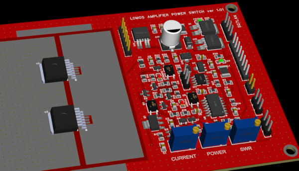
The module has two functions:
The function of distributing the 13.8v voltage, which is used to power the individual amplifier modules. This voltage is independent of the 50V voltage supplying the LDMOS power stage. The 13.8v voltage is taken from the transciver power supply, when the 13.8v transciver power supply is turned on, the voltage appears at the module input. You can choose two modes to start the amplifier:
- the amplifier starts after the 13.8v voltage appears from the power supply.
- the amplifier starts after the transciver is turned on.
This functionality is set by a jumper on the PCB of the module. In case the amplifier starts when the transciver is turned on, it is necessary to connect the amplifier to the ACC jack of the transciver. As I was designing the amplifier for my needs, I took into account the ICOM transcivers I own.
The function of switching off the working voltage of 50v feeding the LDMOS power stage after exceeding the permissible values of SWR, transistor drain current and after exceeding the permissible power generated by the LDMOS transistor
The main executive component is the BTS50085 – Smart Highside High Current Power Switch from Ampleon.
Power Switch BTS50085 acts as an electronic relay or switch to control the flow of current in electrical systems. Being able to control the flow of current based on a control signal, it makes it easy to control the power supply for various devices. Its built-in overvoltage, overheating and short-circuit protection make it a very safe circuit for use in various applications. In addition, due to its low on-resistance, Power Switch BTS50085 is able to enable efficient control of current flow and minimize power loss in the circuit. Therefore, Power Switch BTS50085 is often used in various electronic circuits where current flow control is required, such as in DC-DC converters, power supply circuits, LED lighting and other applications where current flow control is important.
Two or more devices can easily be connected in parallel to increase load current capability.
Basic parameters of the Power Switch BTS50085:
| Output current: | 44A |
| Current limitation: | 90 A |
| On – max resistance: | 9 miliOhms |
| Time on – max: | 400 microseconds |
| Shutdown time- Max: | 110 microseconds |
| Supply operating voltage: | 5 V to 58 V |
| Supply voltage – max: | 58 V |
| Supply voltage – min: | 5 V |
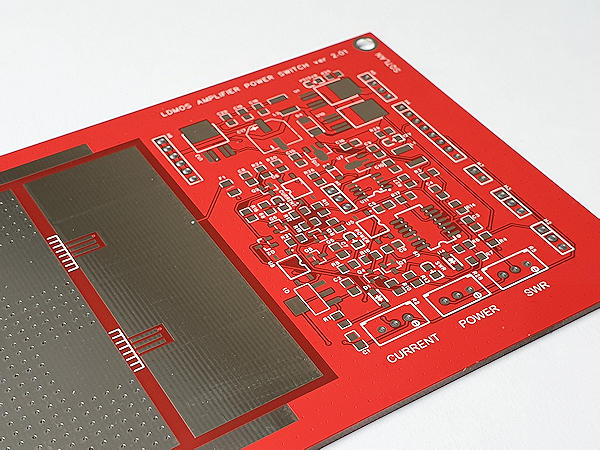
Here is the made PCB, soon will be applied components, mainly SMD …