

The LDMOS (Laterally-Diffused Metal-Oxide-Semiconductor) transistor is a type of MOSFET (Metal-Oxide-Semiconductor Field-Effect Transistor) with lateral field diffusion, which is widely used in RF and microwave applications due to its high power and efficiency.
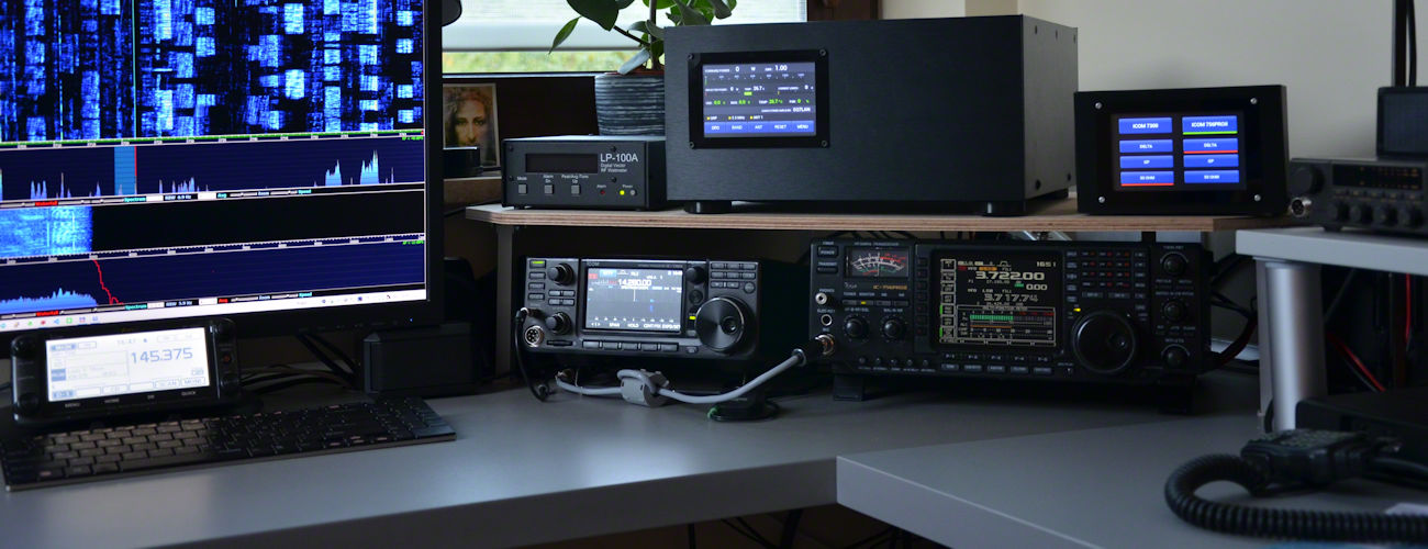
The MRFX1K80 transistor is one example of an LDMOS transistor used in high-frequency applications and features an output power of 1800 W. In brief, the construction of an LDMOS transistor consists of four layers, which are as follows:
- Substrate: The LDMOS transistor consists of a thin, flat piece of silicon, which is the basic substrate material.
- Oxide layer: This layer consists of silicon dioxide and is created by an oxidation process on the surface of the substrate. The oxide layer acts as an electrical insulator between the electrodes and provides protection against substrate damage.
- Channel layer: This layer consists of doped semiconductor material and forms a channel that controls the flow of current between the electrodes. In an LDMOS transistor, the channel layer is laterally diffused, which means that the current flows horizontally rather than vertically, as in traditional MOSFETs.
- Electrodes: The LDMOS transistor has three electrodes: the source electrode, the drain electrode, and the gate electrode. The gate electrode controls the flow of current between the source electrode and the drain electrode.
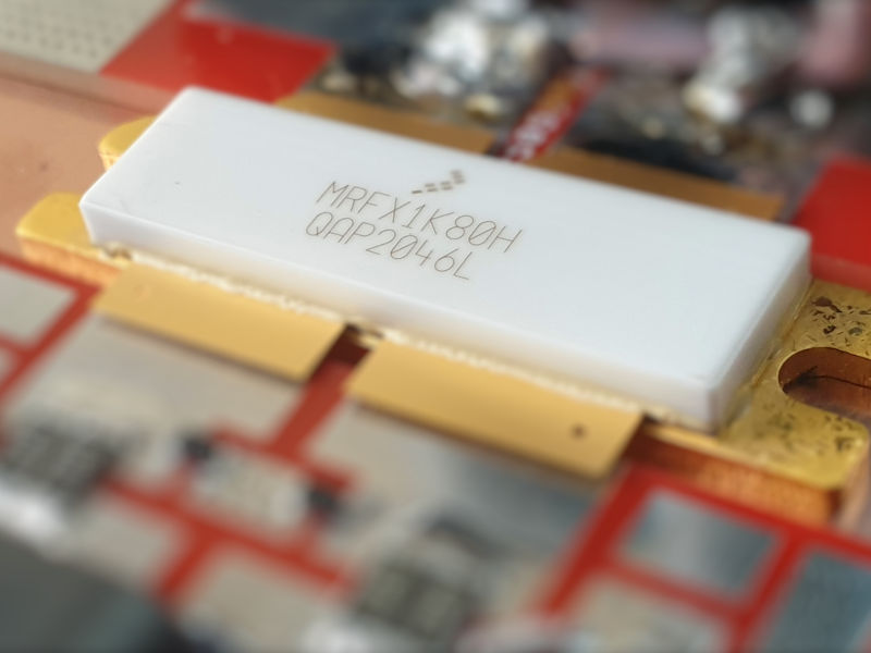
In the case of the MRFX1K80 transistor, it is made using GaN (Gallium Nitride) technology on a SiC (Silicon Carbide) substrate. This combination of materials allows for higher power and efficiency compared to traditional LDMOS transistors.
In the MRFX1K80 transistor, the channel layer is laterally diffused using aluminum (Al) doping and undergoes further diffusion through two diffusion stages, which provides high efficiency. It is worth noting that this transistor requires proper cooling due to the large amount of heat generated during operation.
Capacitance versus Drain–Source Voltage in the ldmos transistor.
The phenomenon of the change in capacitance between the junction of an LDMOS (Laterally Diffused Metal-Oxide-Semiconductor) transistor and its drain with increasing voltage between them is called the “Capacitance versus Drain-Source Voltage” (C-V D-S) effect.
In LDMOS transistors, there are three layers of semiconductor material (two layers associated with the PN junction and a third layer is an insulator, such as silicon dioxide) which together form the PN junction. This third insulator layer isolates the PN junction from the drain of the transistor.
As the voltage between the PN junction and the drain increases, electrons begin to tunnel through the insulator and create a conductive channel, which leads to a change in the capacitance of the PN junction with increasing voltage between the PN junction and the drain of the transistor.
In LDMOS transistors, the capacitance between the PN junction and the drain is usually much larger than in traditional MOSFETs, which is a result of the use of an insulator layer. The C-V D-S effect is significant because it affects the characteristics of the LDMOS transistor in different modes of operation, such as conduction and turn-off modes. In particular, this effect affects the switching speed, response time, and power losses in the transistor.
To minimize the impact of the C-V D-S effect, circuit designers typically use special design techniques such as adjusting the dimensions of the transistor and the PN junction, selecting the proper thickness of the insulator, using additional insulation layers, and other methods that help reduce the capacitance between the PN junction and the drain of the transistor.
Normalized VGS versus Quiescent Current and Case Temperature LDMOS Transistor.
The Normalized VGS versus Quiescent Current and Case Temperature characteristics of an LDMOS (Laterally Diffused Metal-Oxide-Semiconductor) transistor refer to the relationship between the gate-to-source voltage (VGS), quiescent current (IQ), and case temperature (TC) of the transistor.
Quiescent current is the current that flows through the transistor when it is in its “off” state or when no input signal is present. The normalized VGS refers to the gate-to-source voltage that is required to achieve a certain level of quiescent current in the transistor. The case temperature refers to the temperature of the external case of the transistor.
In general, the normalized VGS versus quiescent current curve is a measure of the transistor’s sensitivity to changes in gate voltage. The higher the normalized VGS value, the more sensitive the transistor is to changes in gate voltage.
The case temperature also has a significant impact on the performance of the LDMOS transistor. As the temperature of the transistor increases, its performance characteristics, such as the quiescent current and the normalized VGS, may change. This can affect the overall efficiency and reliability of the device.
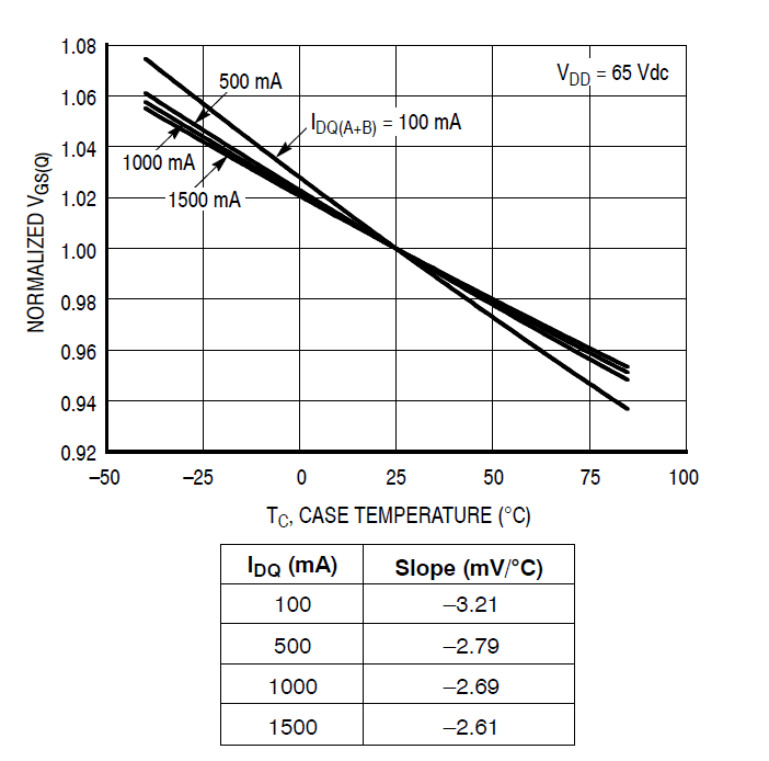
Therefore, it is important to carefully consider the case temperature when designing circuits that use LDMOS transistors. Designers may need to incorporate cooling mechanisms, such as heat sinks or fans, to ensure that the case temperature of the transistor remains within acceptable limits.
In summary, the normalized VGS versus quiescent current and case temperature characteristics of an LDMOS transistor provide important information about its performance and sensitivity to changes in temperature and gate voltage. Careful consideration of these characteristics is necessary for designing circuits that use LDMOS transistors to ensure optimal performance and reliability.